 EN

how-do-forward-bias-and-reverse-bias-affect-diodes-and-leds, how-do-forward-bias-and-reverse-bias-affect-diodes-and-leds, /news
EN
2026/09/25
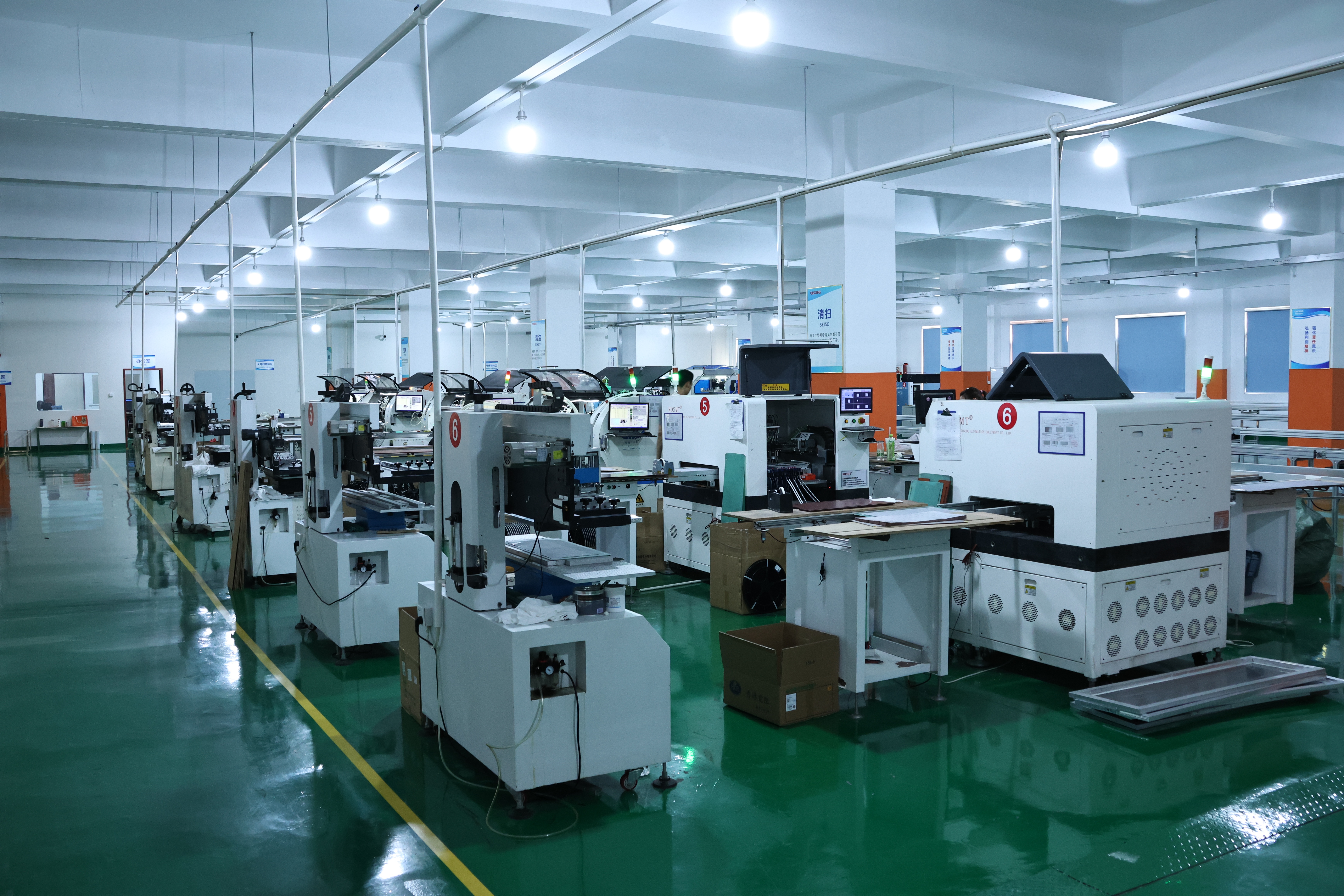
Understanding the behavior of diodes and leds requires knowledge of how electrical bias conditions affect their operation. Forward bias and reverse bias are fundamental concepts that determine whether these semiconductor light emitting devices conduct electricity, emit light, or block current flow. The relationship between applied voltage and device behavior is essential for anyone designing circuits, selecting components, or troubleshooting electrical systems. This article explores how these bias conditions influence diode functionality, light output, and overall system performance.
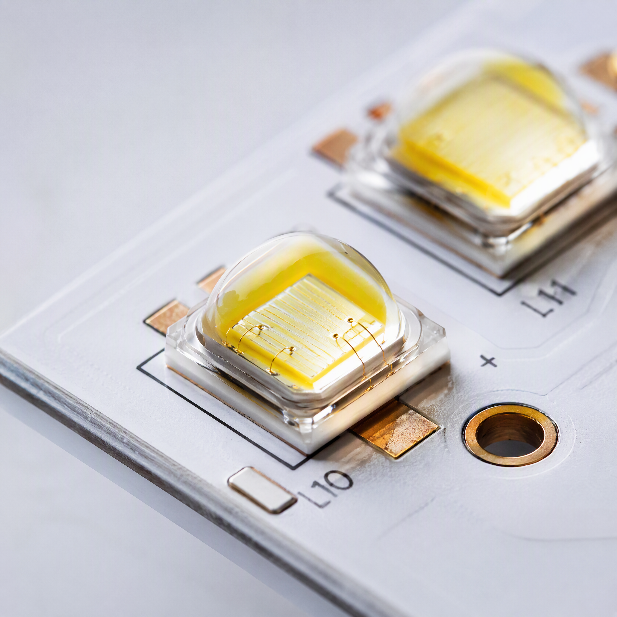
The physics of forward bias and reverse bias operates at the junction between semiconductor materials within diodes and light emitting devices. When positive voltage is applied to the p-side and negative voltage to the n-side, forward bias occurs, allowing current to flow and enabling led efficiency and performance characteristics to become apparent. Conversely, reverse bias applies negative voltage to the p-side and positive to the n-side, restricting current flow and creating a depletion region. Understanding these mechanisms helps optimize semiconductor light emitting devices for specific applications and maximize their reliability in circuits.
Forward bias in diodes and leds occurs when the applied voltage reduces the potential barrier at the junction. The positive side connects to the p-type material and the negative side connects to the n-type material, creating conditions where electrons and holes move toward the junction and recombine. This recombination releases energy in the form of heat or light, depending on the semiconductor material and device type. For semiconductor light emitting devices, this energy release manifests as visible light emission, making forward bias the operational condition for LEDs and other light sources.
When charge carriers recombine within the junction, they transition to lower energy states and emit photons. The wavelength and color of emitted light depend on the semiconductor band gap energy and material composition. Different materials produce different colors: gallium arsenide produces infrared, gallium nitride produces blue and ultraviolet, and aluminum indium phosphide produces red and amber light. The led efficiency and performance of these semiconductor light emitting devices improve significantly when forward bias voltage is optimized for the specific material, ensuring maximum photon generation relative to input current.
Reverse bias creates conditions where the potential barrier at the diode junction increases significantly. The negative voltage connects to the p-side and positive voltage connects to the n-side, pushing charge carriers away from the junction and widening the depletion region. This configuration blocks normal current flow through standard diodes and leds, making the device act as an insulator. The reverse bias condition is crucial for photodiode applications, where diodes and leds designed as sensors must remain reverse biased to detect incoming photons and generate measurable current signals.
At sufficiently high reverse bias voltages, the electric field becomes strong enough to cause impact ionization, where charge carriers acquire enough energy to knock loose additional carriers, creating a cascade effect. This breakdown process can be destructive in standard diodes but is intentionally engineered in Zener diodes to provide voltage regulation. Photodiode applications exploit reverse bias to create a wide depletion region that increases the light detection volume and improves sensitivity to incoming photons. Understanding breakdown voltages and ratings is essential for protecting circuits and preventing damage to semiconductor light emitting devices and photodiodes.
The led efficiency and performance of light sources depends critically on forward bias optimization within safe operating limits. Excessive forward voltage causes increased heat generation and reduced photon output per unit of input current, shortening device life and reducing overall efficiency. Proper current limiting through resistors or current sources maintains the forward bias in an optimal range where light output remains high and thermal stress remains manageable. Quality semiconductor light emitting devices are rated for specific forward voltage and current combinations that maximize led efficiency and performance while ensuring long operational life in practical applications.
Photodiode applications require careful reverse bias management to achieve the desired balance between sensitivity and noise characteristics. Higher reverse bias voltages increase the depletion region width and improve charge collection efficiency, but they also increase dark current and thermal noise. Optimal photodiode performance occurs at reverse bias voltages specified by the manufacturer for particular light detection tasks. The semiconductor light emitting devices designed as sensors must be properly biased during circuit design to deliver accurate photodiode applications in light measurement, optical communication, and imaging systems.
Forward bias applies positive voltage to the p-side and negative to the n-side, reducing the junction barrier and allowing current flow and light emission. Reverse bias applies negative voltage to the p-side and positive to the n-side, widening the depletion region and blocking normal current flow. Forward bias is the operational condition for LEDs producing light output, while reverse bias is used in photodiode applications and voltage regulation circuits.
Proper forward bias voltage maximizes the recombination of charge carriers within the semiconductor light emitting devices, generating maximum photon output relative to input current. Excessive forward bias increases heat generation and reduces led efficiency and performance by causing thermal losses. Optimal forward bias voltage, specified by the manufacturer for diodes and leds, ensures efficient light generation and long device lifespan in practical applications.
Reverse bias in photodiode applications creates a wide depletion region that increases sensitivity to incoming photons and improves charge collection efficiency. The wide depletion width allows more photons to generate electron-hole pairs, maximizing the measurable current signal. Proper reverse bias voltage, as specified for photodiode applications, ensures optimal sensitivity and noise characteristics for light detection in sensors and optical communication systems.
